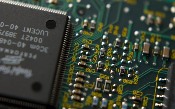
| Wafer Fab & Handling | Litho & Etch Areas | Tool Chamber & Part | Assembly & Test (A&T) | Cleanroom Control | |
|---|---|---|---|---|---|
| Use Cases |
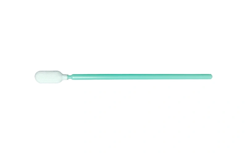
● Wiping FOUPs, cassettes & robot arms ● Removing particles from wafer edge & backside ● Wiping chamber residue after maintenance or process changes |
● Photomask cleaning & daily maintenance ● Cleaning exteriors of steppers, developers & etchers ● Wiping accidental chemical spills |
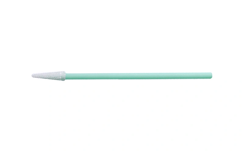
● Periodic cleaning of vacuum chambers, sputtering targets & ion sources ● Removing process by-product deposits from chamber walls & shields ● Detailed part cleaning during preventive maintenance & repairs |
● Cleaning wire bonders, die attach tools & molding dies ● Precision cleaning of test probes & test sockets ● Wiping benchtops, tools & auxiliary equipment in assembly & test areas |
● Wiping cleanroom walls, raised floors, FFU grids & workbenches ● Removing dust from filter grids & return air vents ● Managing spills & daily cleaning in ISO 3-5 cleanrooms |
Semiconductor Series